24/7 Emergency Service
+86 315 6121 218
Contact Us Now!
24/7 Emergency Service
+86 315 6121 218
Contact Us Now!
IR Windows
Parameter
Wafer-level packaging (WLP) is a process of cutting a single infrared detector directly after completing the high-vacuum packaging test procedure on the entire wafer. The main application of infrared technology to the consumer electronics market is miniaturization and low cost, and wafer level packaging can just meet this demand. The wafer-level packaging infrared detector has achieved mass production, and a variety of mature and stable wafer-level infrared movement solutions will open up the emerging application of infrared technology in many fields.
The level of vacuum packaging technology is one of the main factors that determine the cost and reliability of the uncooled infrared focal plane detector. Typical packaging technologies include metal packaging, ceramic packaging, wafer level packaging and pixel level packaging. Among them, metal packaging because of the high cost of metal pipe shell and ceramic pipe shell, and requires a long time of exhaust, its packaging is high cost, production efficiency is low, it is not suitable for large-scale, low-cost production requirements.
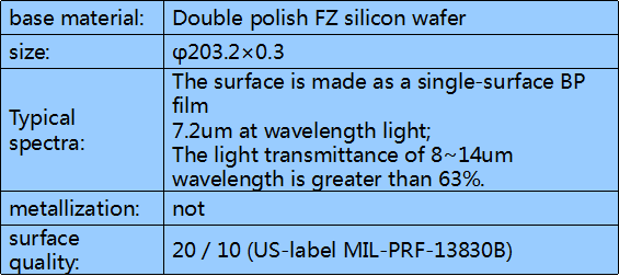
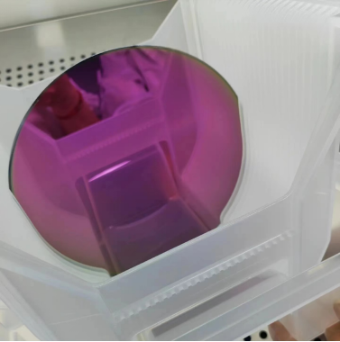
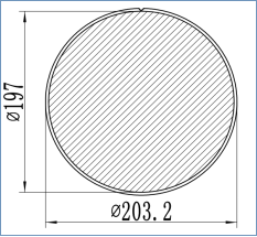
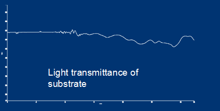
Silicon-based product size: φ 203.2 * 0.3
![]()
![]()
Sounth Easten Road, Linnancang Country, Yutian Town, Tangshan City, Hebei Province, China
+86 138 3893 3595
+86 315 6121 218
Navigation
Follow Us
